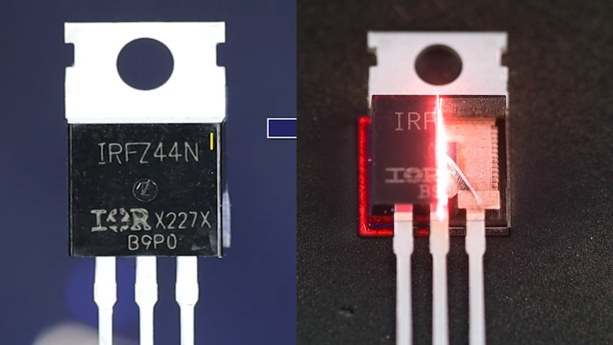
The MOSFET, also known as a metal-oxide-semiconductor field-effect transistor, is a type of FET with an insulated gate that is assembled by the controlled oxidation of that semiconductor. The semiconductor used in it is generally silicon.This ability to change conductivity with the amount of applied voltage can be used for amplifying or switching electronic signals.
source.image: The Engineering Mindset
The MOSFET has 3 terminals, gate, drain and source, differs from BJT which has base, collector, and emitter terminals. By applying voltage to the gate, you create an electrical field that controls the current flow through the channel between the drain and source, without any current flowing from the gate into the MOSFET itself.
The MOS capacitor structure is the heart of the MOSFET. Consider a MOS capacitor where the silicon base is of p-type. If a positive voltage is applied at the gate, holes which are at the surface of the p-type substrate will be repelled by the electric field generated by the voltage applied. At first, the holes will simply be repelled and what will remain on the surface will be immobile (negative) atoms of the acceptor type, which creates a depletion region on the surface. A hole is created by an acceptor atom, e.g. Boron, which has one less electron than Silicon.
Advertisement
Holes aren’t actually repelled, being non-entities; electrons are attracted by the positive field, and fill these holes. This creates a depletion region where no charge carriers exist because the electron is now fixed onto the atom and immobile. As the voltage at the gate increases, there will be a point at which the surface above the depletion region will be converted from p-type into n-type, as electrons from the bulk area will start to get attracted by the larger electric field. This is known as inversion. The threshold voltage at which this conversion happens is one of the most important parameters in a MOSFET.


